Google's move to sell custom TPUs signals a major shift in AI infrastructure. Discover how enterprise architects can move beyond GPU dependency to optimize performance and costs.
The Paradigm Shift in AI Compute Infrastructure
For the past decade, the fundamental blueprint for ai solution architecture for enterprise has been inextricably linked to a single hardware standard: the Nvidia GPU. This monopoly on the underlying compute layer has dictated everything from data center power constraints to the software frameworks developers use to train and deploy machine learning models. However, a structural shift is now underway. Google's unprecedented decision to unbundle its Tensor Processing Units (TPUs) from the Google Cloud Platform and sell the custom silicon directly to rival tech companies and enterprise data centers marks the most significant disruption in AI hardware since the deep learning boom of 2012.
Historically treated as tightly guarded proprietary technology, Google's TPUs are purpose-built Application-Specific Integrated Circuits (ASICs) designed exclusively for the matrix multiplication workloads that underpin neural networks. By allowing external organizations to purchase this hardware as a capital expenditure (CapEx) rather than renting it as an operating expense (OpEx) through the cloud, Google is directly attacking Nvidia's 75% gross margins and its $4.39 trillion market capitalization medium.com.
This is not merely a vendor swap; it is a fundamental architectural divergence. As frontier models like Anthropic's Claude 4.5 Opus and Google's own Gemini 3 demonstrate that state-of-the-art AI can be trained entirely outside the Nvidia ecosystem, enterprise architects must reevaluate their infrastructure roadmaps. This deep dive explores the technical architecture of Google's latest TPU generations, the software abstraction layers breaking the CUDA lock-in, and the economic forces driving the commoditization of AI compute.
The Architectural Divergence: Generalists vs. Specialists
To understand why Google's hardware pivot is so threatening to the status quo, one must examine the silicon-level design philosophies that separate Graphics Processing Units (GPUs) from TPUs.
Nvidia's GPUs are the Swiss Army knives of the computing world. They are miraculous feats of engineering designed to handle a vast array of parallel processing tasks: rendering high-resolution video game graphics, running complex physics simulations, mining cryptocurrency, and training large language models (LLMs). Because they are built to do everything, they carry the silicon overhead required for everything.
When an enterprise purchasing high-end Nvidia GPUs deploys them for AI inference, a significant percentage of the chip's die space—which includes rasterization cores, ray-tracing hardware, and general-purpose logic—remains dark or underutilized.
"When you are training a frontier model like Gemini or Llama 3, you need the raw, flexible power of NVIDIA. But once that model is trained and served to millions of users (inference), using a GPU is capital inefficiency at its finest." — gjgalante.medium.com
Google's TPUs, conversely, are uncompromising specialists. They are designed from the ground up for one specific mathematical operation: matrix multiplication, the core mathematical operation of deep learning.
The architectural heart of a TPU is the Systolic Array. Unlike a traditional CPU or GPU, which must constantly read from and write to registers and caches for every calculation, a systolic array passes data seamlessly through a grid of Arithmetic Logic Units (ALUs). Data flows in waves (systoles, akin to a heartbeat) through the array, performing thousands of multiply-accumulate (MAC) operations in a single clock cycle without the power-hungry overhead of continuous memory access.
This ASIC philosophy yields massive dividends in performance-per-watt and cost-per-FLOP. By stripping away the general-purpose logic, Google can pack more matrix multiplication units onto a smaller, cheaper-to-manufacture die, fundamentally altering the unit economics of AI execution.
Deep Dive: The Ironwood (TPUv7) System Architecture
Google's TPU roadmap has evolved rapidly over the past 24 months, culminating in the deployment of two distinct architectural tracks: the Trillium (v6) series, which offers a 4-5x performance uplift over previous generations for general training, and the newly unveiled Ironwood (v7 / TPU7x) architecture datacenterfrontier.com.
Ironwood represents a masterclass in system-level engineering, designed specifically to tackle the massive computational demands of the "age of inference" and scale-out training.
The Supercomputer Pod
The fundamental unit of compute in the Google paradigm is not the individual chip, but the Pod. As Val Bercovici, Chief AI Officer at WEKA, noted, TPUs are "designed as a complete 'system' rather than just a chip" venturebeat.com.
An Ironwood pod consists of 9,216 interconnected TPU chips. Operating in unison, a single pod delivers more than 40 exaFLOPS of dense FP8 (8-bit floating point) compute. This scale is achieved not just through faster silicon, but through a revolutionary approach to data center networking.
Inter-Core Interconnect (ICI) and Optical Switching
The primary bottleneck in distributed AI training is rarely the processor's speed; it is the network. Moving petabytes of gradient updates and model weights between thousands of chips creates immense latency. Nvidia solves this with its proprietary NVLink and InfiniBand networking fabrics, which are highly performant but exceptionally expensive.
Google bypasses standard networking topologies entirely within the pod. TPUs communicate via a custom Inter-Core Interconnect (ICI). In the Ironwood architecture, Google leverages proprietary Optical Circuit Switches (OCS). Instead of converting electrical signals to optical, routing them through traditional packet switches, and converting them back, OCS uses microscopic mirrors (MEMS) to bounce light directly from one fiber to another.
This optical fabric allows the 9,216 chips in an Ironwood pod to dynamically reconfigure their network topology on the fly, optimizing the physical network paths to match the specific data flow of the neural network being trained. The result is a near-linear scaling efficiency that treats a massive cluster of chips as a single, coherent supercomputer, dramatically reducing the "compute tax" associated with distributed training.
Memory Bandwidth and the Inference Bottleneck
For AI inference—particularly for autoregressive LLMs generating text token by token—the bottleneck shifts from compute to memory bandwidth. The model's weights must be continually loaded from High Bandwidth Memory (HBM) to the processor. Ironwood addresses this with tightly integrated, next-generation HBM3e and an expanded SRAM pool directly on the die, allowing larger batch sizes and drastically reducing the latency of the Key-Value (KV) cache retrieval critical for long-context windows.
The Software Counter-Offensive: Defeating the CUDA Moat
Hardware superiority is meaningless without the software to utilize it. For over a decade, Nvidia's ultimate defense has been CUDA (Compute Unified Device Architecture). Millions of AI researchers and engineers have built their pipelines, custom kernels, and optimization libraries on CUDA. Switching to a new hardware platform traditionally meant rewriting years of code—a prohibitively expensive proposition known as the "CUDA moat."
Google's strategy to bridge this moat relies on a powerful combination of high-level mathematics and low-level compiler magic: JAX and XLA.
JAX: The Mathematical Abstraction
JAX is a high-performance numerical computing library developed by Google. To a developer, writing in JAX feels almost identical to writing in NumPy, the standard Python library for data science. However, JAX is designed from the ground up for machine learning. It supports automatic differentiation (calculating the gradients needed for neural network training) and is hardware-agnostic.
Developers write their model architectures in JAX (or frameworks built on top of it, like Flax), completely abstracted away from the underlying hardware. The code does not know or care whether it will run on an Intel CPU, an Nvidia GPU, or a Google TPU.
XLA: The Compiler Engine
The translation from high-level math to optimized silicon execution is handled by XLA (Accelerated Linear Algebra). XLA is a domain-specific compiler that takes the computational graph generated by JAX (or PyTorch via PyTorch-XLA) and compiles it into highly optimized machine instructions.
When XLA targets a TPU, it performs aggressive optimizations that are difficult to achieve manually:
- Operator Fusion: In standard execution, a model might calculate a matrix multiplication, write the result to memory, read it back, apply an activation function (like ReLU), write it back, read it again, and apply a dropout layer. XLA analyzes the graph and "fuses" these operations. The data stays in the TPU's ultra-fast SRAM, passing through the matrix multiplier, the activation unit, and the dropout unit in a single continuous flow before being written back to main memory. This drastically reduces memory bandwidth starvation.
- Memory Layout Optimization: XLA dynamically restructures how tensors are physically laid out in the HBM to ensure the systolic arrays are fed with data at maximum efficiency, minimizing idle clock cycles.
By heavily investing in the PyTorch-XLA bridge and the JAX ecosystem, Google has made the hardware layer transparent. Enterprise AI teams can now port massive PyTorch models from Nvidia clusters to TPU pods with minimal code changes, effectively neutralizing the CUDA lock-in.
The Economics of Unbundling: CapEx vs. OpEx
The technical brilliance of the TPU is only half the story; the real disruption lies in Google's go-to-market strategy.
Until recently, the only way to access a TPU was to rent it by the hour via Google Cloud Platform (GCP). This OpEx model is highly profitable for cloud providers but increasingly punitive for large-scale AI developers and hyperscalers. When a company is running tens of thousands of accelerators 24/7 for months to train a frontier model, the "cloud tax"—the premium paid over the raw hardware cost—becomes astronomical.
By unbundling the TPU and offering it directly to external customers as a hardware purchase (CapEx), Google is fundamentally altering the data center supply chain newscientist.com.
The Hyperscaler Rebellion
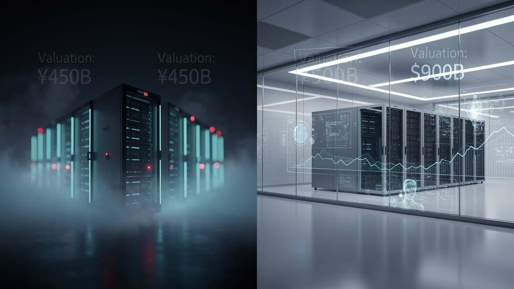
Companies like Meta, Microsoft, and Amazon are spending tens of billions of dollars annually on AI infrastructure. In 2023 and 2024, the vast majority of this capital flowed directly to Nvidia.
However, market reports indicating that Meta is exploring shifting billions in infrastructure spending toward Google's TPUs highlight a critical inflection point gjgalante.medium.com. Hyperscalers and large enterprises are desperate for leverage against Nvidia's pricing power. By offering a viable, high-performance alternative that can be physically installed in a customer's own data center, Google is providing that leverage.
Furthermore, Google's manufacturing alliance with Broadcom and TSMC ensures a robust supply chain capable of producing these specialized ASICs at scale, at a lower per-unit cost than Nvidia's massive, complex GPU dies.
Frontier Validation: The Proof in the Silicon
The ultimate test of any AI hardware is its ability to train and serve frontier-class models. The industry has long operated under the assumption that achieving state-of-the-art performance required massive clusters of Nvidia H100 or Blackwell GPUs.
That narrative has been definitively shattered. Two of the most capable multimodal AI models in existence—Google's Gemini 3 and Anthropic's Claude 4.5 Opus—were trained entirely on Google's Ironwood TPUv7 infrastructure venturebeat.com.
Anthropic's decision to utilize TPUs for its flagship model is particularly telling. As an independent AI lab heavily backed by Amazon (which has its own custom silicon, Trainium) and reliant on massive compute resources, Anthropic's selection of the TPUv7 validates both the hardware's raw performance and the maturity of the XLA/JAX software stack. It proves that the largest, most complex distributed training runs in the world can be executed flawlessly outside the CUDA ecosystem.
Redesigning Enterprise AI Architecture
For technology decision-makers, CTOs, and systems architects, Google's entry into the hardware sales market demands a strategic pivot in how AI data centers are designed, provisioned, and managed. The era of homogeneous, GPU-only clusters is ending, giving way to heterogeneous compute environments.
1. Workload Segmentation
Enterprises must stop treating AI compute as a monolithic requirement. The architecture of the future relies on workload segmentation:
- Exploratory Research and Prototyping: General-purpose GPUs remain valuable for highly experimental architectures, custom CUDA kernel development, and workloads that require frequent, unpredictable changes to the underlying math.
- Scale-Out Training: For training massive transformer models on static architectures, TPU pods (like Trillium and Ironwood) offer superior linear scaling and lower interconnect latency.
- High-Volume Inference: For serving models in production, specialized inference ASICs (like Ironwood's inference configurations) provide vastly superior throughput-per-watt, drastically lowering the cost of goods sold (COGS) for AI application providers.
2. Infrastructure as Code and Hardware Agnosticism
To take advantage of hardware commoditization, enterprise AI architectures must be strictly hardware-agnostic. This requires standardizing on frameworks like PyTorch and utilizing compilers like XLA or OpenAI's Triton. DevOps and MLOps pipelines must be designed so that a model can be trained on a cloud-based GPU cluster on Monday and deployed for inference on an on-premise TPU pod on Friday, with zero changes to the core model code.
3. Power Density and Data Center Design
The physical footprint of AI is changing. While Nvidia's Blackwell GPUs push the limits of power consumption (exceeding 1000W per chip and requiring complex liquid cooling solutions), TPUs' stripped-down ASIC design generally offers higher compute density per watt. However, deploying a TPU pod requires specific infrastructure, particularly regarding the Optical Circuit Switches and the physical fiber routing required for the ICI network. Enterprises opting to purchase TPUs will need to adapt their data center floor plans and cooling architectures to support these tightly coupled, pod-scale systems.
Conclusion: The Commoditization of Intelligence
The AI industry is maturing from a phase of algorithmic discovery into a phase of industrial-scale manufacturing. In this new era, compute is the raw material, and efficiency is the ultimate competitive advantage.
Google's decision to sell custom TPUs directly to the market is not just an attack on Nvidia; it is a catalyst for the commoditization of AI hardware. By breaking the monopoly on high-performance accelerators and proving that the CUDA moat can be bypassed with intelligent compiler design, Google is driving down the fundamental cost of artificial intelligence.
For enterprise architects, the message is clear: the infrastructure of the future will not be defined by loyalty to a single vendor, but by the ability to orchestrate heterogeneous compute resources across a hardware-agnostic software stack. The "one chip to rule them all" era is over; the era of optimized, purpose-built AI infrastructure has officially begun.
Last reviewed: April 7, 2026